Transistor PA RF Output Power vs Load
Impedance
Grant Bingeman, P.E.
This is an article based primarily on empirical evidence, and is not the
usual theoretical treatment of the subject of PA design, although it is in full
agreement with the laws of physics. As such I think you will find it offers some
fresh information in the spirit of amateur radio and experimentation, and will
be of particular interest to QRP (10 watts SSB, 5 watts CW) aficionados.
Conventional wisdom asserts that the RF power output level from a transmitter
is optimal when the impedance presented to the power amplifier is closest to its
design center value. An RF output network serves to transform the typical 50 ohm
load impedance to this desired PA value. But what happens when your antenna
presents something other than 50 + j0 ohms to your transmitter? Most of us are
aware that a transmitter load impedance specification often simply refers to a
maximum tolerable VSWR value. Since there are an infinite number of impedances
that fall within the typical load VSWR tolerance specification of 2.0, one might
ask the question, "are some of these impedances better than others?" This
article will discuss specifically how much the measured PA efficiency and
RF power output level from an MFJ 9420 vary over a large set of impedances other
than 50 ohms resonant, and what this means to your received signal strength. If
QRP is defined as 10 watts PEP for SSB operation, it would be good to know if
certain loads caused the PA to deliver more than 10 watts. For example, if you
are working towards a QRP Worked All States award, but some of your QSLs were
made at 11 watts, how would you feel?
The MFJ 9420 is a CW and SSB "travel radio" rated at 10 watts PEP, tuned to
the 20 meter amateur radio band. Its PA consists of an MRF477 transistor
operating single-ended class AB. This heat-sinked transistor is capable of
dissipating 80 watts, so is not in much danger of burning up in this
application, which is probably why the load VSWR spec for this radio is a
relatively high 3.0. The output network of the 9420 consists of a 1:4
transformer followed by two 50:50 ohm, -90 degree pi networks (Figure 1). Thus a
50 ohm resistive load presents about 12.5 ohms to the PA. Since the phase shift
across the output network is 180 degrees, any impedance at the output of the
transmitter appears as that same impedance divided by 4 at the collector of the
transistor (impedances repeat every 180 degrees on a lossless transmission
line). This is a relatively broad-band output network, and behaves pretty much
the same across the entire amateur radio 20 meter band from 14.0 to 14.35 MHz.
By contrast, class C amplifier output networks have a much higher Q and tend to
have a narrower bandwidth. Some amateur radio CW transmitters use a class C RF
amplifier.
Usually there is some collector-to-emitter capacitance built into the PA
transistor, and if this is greater than that required by the output network, it
has to be parallel-resonated with an inductance, or otherwise accounted for in
the design. According to the Motorola published data, the MRF477 can be modeled
as about 1300 pF in parallel with 2.2 ohms when delivering 40 watts at 14.2 MHz,
but since the MFJ 9420 PA is operating at only 10 watts PEP nominal, the actual
parallel equivalent circuit for this condition is not specified. However the
self inductance of the 1:4 transformer will tend to offset the collector
capacitance, so we might assume for the moment that these "stray" reactances
wash each other out, just to keep things simple. Besides, best PA performance
may not occur exactly at resonance anyway. There is often a compromise between
distortion, power output and efficiency.
The MRF477 is a bipolar NPN silicon transistor, or BJT. If it were an FET, it
might tend to behave as a tetrode or current source. Bipolar transistors on the
other hand are said by some to behave as a triode or voltage source, although
they may be modeled best as an exponential voltage-controlled current source in
Spice analysis. Many models assume that there are no power supply limits, and no
feedback, deliberate or stray. However in the real world there is not much
headroom designed into a transmitter power supply, because unnecessary headroom
wastes money. During these tests I used a big power supply that actually cost
more than the transmitter under test, but at least I knew its current rating and
voltage regulation were not going to taint the results. So keep in mind that you
may get different results with an economical power supply, or with a different
type of RF power transistor. And RF feedback can very significantly alter the
behavior of a PA as the load is varied. But the main point of this article is
that, rather than relying on theoretical device models, I decided to
measure the PA performance of my MFJ 9420.
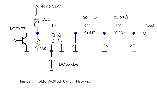
The PA has a 150 ohm
stabilizing or damping resistor directly across the primary of the transformer,
which pulls the 12.5 ohms down to about 11.5 ohms. This means that about 8
percent of the PA output power is wasted in the damping resistor, and 92 percent
is delivered to the output network. This is a small price to pay for parasitic
suppression under variable load conditions. It means that spurious emissions are
minimized and PA stability is enhanced, reducing the chances of over-dissipation
and failure of the transistor when operating into mismatched loads.
With no load whatsoever attached to the transmitter, I measured a PA DC
current of 0.4 amps when using a 13.6 VDC supply. I ran it for 30 seconds with
no problems, but would not recommend this as a common practice with other
transmitters where the transistor might be running closer to its maximum
ratings, or where an open-circuit at the output of the transmitter may reflect
as a short-circuit at the PA (when overall output network phase shift is near an
odd multiple of 90 degrees).
The PA RF choke in the power supply lead has about 0.6 ohms of DC resistance.
With the key down and 13.6 volts supplied to the 9420, the RF power delivered to
a 47 - j10 ohm load is about 9.0 watts. The stray reactances between the UHF
connector and the printed circuit board transform this to about 48 - j5 ohms at
the last capacitor in the output network. The DC input current to the radio is
about 1.64 amps under these conditions, of which 0.12 amps is the quiescent
current with the key up, and 0.23 amps is the current drawn by the oscillator
and driver stages. This leaves 1.29 amps delivered to the PA, which means the
voltage drop across the RF choke is about 0.8 volts, leaving 12.8 volts across
the PA transistor. Thus the transistor input power is 12.8 volts times 1.29
amps, or about 16.5 watts, yielding an efficiency of about 54 percent at 14.25
MHz, which includes output network and damping resistor losses. If you count the
loss in the choke, about 1.0 watts, the overall PA efficiency is a bit lower,
about 51 percent. For the remainder of this article I will include the choke
losses in the PA efficiency figures. But 51 percent is not bad for a practical
class AB HF amplifier
The insertion loss of the DC ammeter in series with the PA RF choke was
accounted for in the data collection. The voltage drop across this meter was
almost small enough to ignore (about 0.2 volts), but I corrected the results
anyway. Note that the PA bias and all other parameters were left at the factory
settings through-out the testing. Using an attic dipole 30 feet off the ground,
this particular 9420 received excellent SSB signal reports in Italy and Brazil
from its Dallas QTH in April 1998, so the factory settings must be okay.
The power delivered to the load was determined by measuring the peak-to-peak
value of the RF waveform across the resistive portion of the load with an
oscilloscope, dividing this value by 2.82 to convert from peak-to-peak to RMS,
squaring the result, then dividing this number by the load resistance (Equation
1). The ground side of the scope probe was always attached to the grounded side
of the resistor in the load. The reactive component in the load was floating.
The impedances were measured with a Hewlett Packard vector impedance meter
calibrated to an NBS standard. The oscilloscope was recently calibrated in an
ISO9001 lab, and its accuracy was better than two percent. In terms of measured
power, this means that the accuracy was better than about four percent.
P = (V / 2.82 )2 / R Equation 1
The following data (Table 1) were taken with a constant 13.6 volts DC
supplied to the transceiver. Note that many 13.8 volt supplies are not very well
regulated, and often the cable between the supply and the transceiver has a
significant voltage drop across it as well when the key is down, especially if
there is an in-line fuse. When using a portable battery pack, there will also be
some sag in the voltage unless it is a large fully-charged battery, or a good
voltage regulator is built into the battery pack. The 9420 uses a number of
voltage regulators on its printed circuit cards, but the PA is connected
directly to the 13.8 volt DC input and has no voltage regulation. The 9420 is
designed to operate over a supply voltage range of 12 to 15 VDC. There is no
series protective diode, only a shunt crowbar diode and a fuseable printed
circuit trace, so be careful not to hook up your power supply leads backwards!
If you add a conventional fuse, you may find that you lose half a watt in its
resistance when the key is down.
TABLE 1
load PA
input PA input resistor RF load
PA
impedance VSWR current
power voltage power
effic. relative field
19 + j8 ohms
2.71 1.65 A 22.4 W 30
Vpp 6.0 W 27 % 82
% -1.7 dB
28 + j8 1.85
1.41 19.2
40
7.2 38
89 -1.0
34 +
j8 1.54
1.35 18.4
44
7.2 39
89 -1.0
41 +
j8 1.30
1.16 15.8
50
7.7 49
92 -0.7
47 +
j8 1.22
1.09 14.8
53
7.5 51
91 -0.8
56 +
j8 1.21
1.03 14.0
56
7.0 50
88 -1.1
68 +
j8 1.40
0.95 12.9
58
6.2 48
83 -1.6
82 +
j8 1.66
0.84 11.4
63
6.1 53
82 -1.7
100 +
j8 2.02
0.79 10.7
66
5.5 51
78 -2.2
120 +
j8 2.41
0.72 9.8
65
4.4 45
70 -3.1
150 +
j8 3.01
0.67 9.1
68
3.9 43
66 -3.6
28 -
j10 1.89
1.65 22.4
40
7.2 32
89 -1.0
34 -
j10 1.57
1.55 21.1
48
8.5 40
97 -0.3
41 -
j10 1.34
1.33 18.1
54
8.9 49
99 -0.1
47 -
j10 1.24
1.29 17.5
58
9.0 51
100 0.0 ref
56 -
j10 1.25
1.18 16.0
58
7.6 48
92 -0.7
68 -
j10 1.35
1.00 13.6
59
6.4 47
84 -1.5
82 -
j10 1.68
0.85 11.6
62
5.9 51
81 -1.8
100 - j10
2.03 0.82
11.2 65
5.3 47
77 -2.3
120 - j10
2.42 0.75
10.2 64
4.3 42
69 -3.2
150 - j10
3.02 0.65
8.8 66
3.7 42
64 -3.9
33 -
j43 2.96
1.47 20.0
43
7.0 35
88 -1.1
47 -
j43 2.37
1.30 17.7
51
6.4 36
84 -1.5
56 -
j43 2.22
1.14 15.5
53
6.3 41
84 -1.5
68 -
j43 2.18
1.04 14.1
55
5.6 40
79 -2.0
33 +
j53 3.60
0.67 9.1
30
3.4 37
61 -4.3
47 +
j53 2.85
0.71 9.7
40
4.3 44
70 -3.1
56 +
j53 2.64
0.69 9.4
44
4.3 46
71 -3.0
68 +
j53 2.53
0.70 9.5
49
4.4 46
71 -3.0
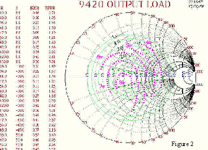
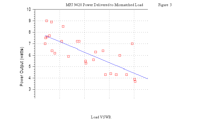
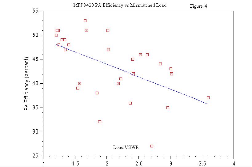
We can draw some general conclusions from these data. First of all one can
see that the general trend per Figures 3 and 4 is towards lower power output and
efficiency with increasing VSWR. It also appears that for a given VSWR, power
output degrades less when the load resistance is lower than the nominal 50 ohms.
However, PA efficiency and heating are both worse on this low resistance side of
the Smith chart (Figure 2). I sketched in some rough constant-power curves on
the Smith chart, but more data points would be required to plot these
accurately. These curves form concentric rings around the maximum power output
location, which is generally at the center of the Smith chart.
All of the data tend to indicate that the PA is behaving more as a voltage
source than as a current source, but it is clearly not an ideal voltage source.
A very stiff voltage source would produce four times as much power in a 25 ohm
resistive load as it produced in a 100 ohm load. And at first glance I don't see
an obvious constant source impedance value that would account for the measured
results either, or that such a linear source impedance even has to exist.
Note that the correlation of PA power dissipation and efficiency with load
resistance is true both at the output of this transmitter and right at the PA,
since the phase shift across this network is 180 degrees lagging. Therefore you
could probably extrapolate this relationship to other transmitters using other
output networks, if they used the same type of PA. For example, you would expect
the opposite effect to occur in a transmitter having a -90 degree or -270 degree
output network. That is, a high output load resistance would reflect as a low PA
load resistance in such a transmitter, which could result in possible
over-heating of the PA. The idea is to translate the load impedance from the
output of the transmitter to the PA, keeping in mind that a low PA load
resistance is going to stress the PA more than a high load resistance, at least
in the MFJ 9420.
By the way, here is a trick question. Which load has a lower VSWR in a 50 ohm
system: 50 + j40 ohms or 70 + j40 ohms? Did you think it was the load with the
resistance closest to 50 ohms? The correct answer is 70 + j40, which has a VSWR
of 2.09, as opposed to 2.18 for the 50 + j40 ohm load. Which load is better for
your transmitter, assuming you don't have an adjustable impedance matching
network between these loads and your PA to compensate for the mismatch? Well,
you are probably going to have to measure your transmitter RF power output,
input power, inter-modulation distortion and spurious RF content to fully answer
that question, since all these performance criteria will vary from one
transmitter to the next.
You can get a reasonable idea of the power delivered to your load by
subtracting the reflected power reading from the forward power reading of your
directional coupler. By the way, when was the last time you verified the
accuracy of your power meter, or calibrated the impedance of your dummy load?
Chances are your reflectometer, or directional-coupler, or magni-phase, or
power-meter, or SWR-meter may only provide reasonable accuracy for loads close
to 50 ohms. I also measured a commercial "50 ohm" ham radio load as 56 + j0 ohms
at 14.25 MHz, so when in doubt, be sure to measure. A commercial dummy load may
be specified as having a VSWR of 1.2 over a fixed frequency range, and may never
present 50 + j0 ohms at any frequency.
You can also determine the delivered power to your load as I2R
assuming you have an accurate RF ammeter and impedance measuring device, or as
V2/R assuming you have an accurate RF voltmeter or oscilloscope. A
calorimetric load is used by professional transmitter manufacturers, designers
and broadcasters when they want a really accurate measurement of RF power
output, and this requires accurate coolant flow and temperature measurement, not
to mention knowledge of the specific gravity of the coolant, or humidity if the
coolant is air, etc.
Unprocessed single sideband voice modulation requires less average current
from the power supply than tone modulation or typical morse CW, so the PA may
produce higher peak transient power outputs for SSB voice than for CW, unless
your power supply is very well regulated. If the power supply voltage regulation
is reasonably stiff and its current rating is conservative, the peak envelope
power and CW output power may be the same. You can consider the PEP value to be
the CW value over one RF cycle at the maximum level of modulation. Normal voice
transients don't stick around long enough to cause the typical power supply to
sag as much as it will during a key-down situation. Have you ever measured the
DC voltage supplied to your PA while the key is down or your modulation density
is high? How much does it sag? You might be surprised.
Since the radiated field intensity is proportional to the square-root of the
power output from your transmitter, a receiver would hardly see any change in
signal strength from a 9420 operating into the full range of loads within a 3.0
VSWR circle on the Smith chart according to Table 1. One S unit is typically
considered to be 6 dB, and the worst relative field for the 3.0 VSWR circle data
in Table 1 is 64 percent or -3.9 dB. Therefore one might conclude that as long
as the reduced PA efficiency and stability are tolerable, why worry about
matching the load impedance down to the nit? If you are voice modulating, the
average modulation depth is relatively light compared to some other modes, and
the duty cycle of a normal QSO allows the PA to cool quite a bit between
transmissions. Of course, if your chosen mode has a high modulation density and
high duty cycle, then you should be more concerned about mismatch. But in the
case of the 9420's MRF477 PA, even with the worst-case 3.0 VSWR load you will
not be operating near the power dissipation rating of this transistor.
But there are other performance considerations related to load impedance. For
example, will the radio be able to modulate cleanly and fully if the power
supply is already taxed by poor PA efficiency? If RF audio processing is used,
will the feedback sample be degraded by a poor load? Will PA stability be okay
without modulation, but degenerate with modulation when a poor load is present?
When in doubt, play it safe and match that impedance.
Keep in mind that Class C and D RF power amplifiers behave quite differently
from Class AB amplifiers, and every class AB transmitter has a different output
network, so be careful that you don't indiscriminately apply the information
contained in this article to an amplifier operating with a different amount of
bias or a different set of filters and impedance matching networks.
So in conclusion it appears that when the VSWR of the load impedance
presented to an MFJ 9420 is kept below 3.0, then the worst reduction in signal
strength one can expect is about four dB, which is less than one S unit. Some
additional good news is that if you define 10 watts PEP as an official QRP level
for SSB, then you will probably never violate this limit by operating a 9420
into a mismatched load. Admittedly Figure 3 is not a terribly scientific plot of
all the possible load impedances, but it does show a general trend to lead one
to the conclusion that 10 watts output is only possible when the load is close
to a perfect match and the power supply voltage is near 13.8 volts. The maximum
RF power output I recorded was 9.0 watts for a power supply voltage of 13.6 VDC
and a not quite perfect impedance match. If we assume that 10 watts is possible
with a perfect match at 13.8 volts, this scales to about 12 watts at 15.0 volts,
the allowed supply voltage upper limit. If we assume that the accuracy of my
measurements in a worst-case scenario might be as poor as +/- ten percent of PA
output power, then it might be possible to violate the 10 watt QRP limit under
certain conditions. If you really want to ensure that you stay below 10 watts,
crank back the supply voltage enough to allow some headroom for the resolution
and accuracy of your test equipment, just in case it might be reading a bit low.
I invite the reader to make his own set of PA performance measurements for
various load conditions, and it would not surprise me if there were certain
loads that yielded a PA output power greater than that obtained with the nominal
50 ohm resonant condition in other transmitters. Of course this will depend on
the power supply performance, the RF output network, the type of PA
transistor(s) and feedback, etc. But I think if you characterize your
transmitter's PA performance with an empirical set of data such as I did for my
little 9420, then you will know exactly what to expect. And if you are operating
QRP or looking for extra points in a contest by staying below a certain power
level, it is nice to know under what RF load conditions you might get
disqualified!
Grant Bingeman, KM5KG, is a Principal Engineer with Continental Electronics
in Dallas, Texas, where they design and manufacture high power transmitters and
antennas from DC to light. Grant has published over 100 technical articles in
various professional and trade journals. His e-mail address is
DrBingo@compuserve.com. This particular article has been published in the RSGB
February 1999 RadCom issue.